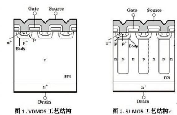
For the conventional VDMOS device structure, the contradictory relationship between Rdson and BV should be improved by reducing the EPI impurity concentration. However, the epitaxial layer is also a channel for the forward current flow. As the EPI impurity concentration decreases, the resistance will inevitably increase and Rdson will increase. Rdson directly determines the loss of MOS monomer. Therefore, for ordinary VDMOS, the contradiction between the two is irreconcilable, which is the limitation of conventional VDMOS. For COOLMOS, however, this contradiction is not so obvious. By setting a P-block deep into the EPI, the BV is greatly improved, while having no effect on Rdson. For conventional VDMOS, reverse voltage resistance mainly depends on PN junction at the interface between N-type EPI and body region. For a PN junction, voltage resistance mainly depends on the endurance of the depletion region, the size of the electric field in the depletion region and the area of the width of the depletion region. The concentration of conventional VDSMO and P body is greater than that of N EPI. It should also be clear that the depletion region of PN junction mainly diffuses to the side with low impurity. Therefore, under this structure, the expansion of the depletion region on the side of P body region is very small, which basically does not contribute much to the pressure. The electric field intensity in this region changes gradually. The closer the area is to the PN junction plane, the greater the electric field intensity E is. For COOLMOS structure, due to the setting of a P region with a lower concentration of P body, the depletion region at one side of P region is greatly extended, and this region is deep into EPI, resulting in both sides of PN junction can withstand high voltage. In other words, the peak electric field Ec is shifted from close to the device surface. It's moving deeper into the device.

Cool-MOS advantage
1. Small on-state impedance and small on-state loss.
Since the Rdson of SJ-MOS is much lower than that of VDMOS, the on-off loss of SJ-MOS in system power products must be much less than that of VDMOS. It greatly improves the on-off loss of the single MOSFET on the system product and improves the efficiency of the system product. This advantage of SJ-MOS is particularly outstanding in the power supply products with large power and large current.
2. With the same power specifications, the package is small, which is conducive to the improvement of power density.
First of all, under the condition of the same current and voltage specifications, the crystal source area of SJ-MOS is smaller than that of VDMOS process. In this way, as a MOS manufacturer, products of the same specifications can be packaged with relatively small volume, which is conducive to the improvement of power density of the power supply system.
Secondly, due to the reduction of the on-off loss of SJ-MOS, the loss of power supply products is reduced, because these losses are dissipated in the form of heat. In practice, we often increase the radiator to reduce the temperature rise of MOS monomer, so as to ensure that it is within the appropriate temperature range. Because SJ-MOS can effectively reduce the heat, reduce the volume of the radiator, for some slightly lower power supply, even the use of SJ-MOS after the radiator can be completely removed. Effectively improve the power density of the system power supply products.
3. The grid charge is small, and the driving ability of the circuit is reduced.
The gate charge of traditional VDMOS is relatively large, we often encounter the temperature rise problem caused by the insufficient driving capacity of IC in practical applications, some products in the circuit design in order to increase the driving capacity of IC, to ensure the fast conduction of MOSFET, we have to increase the push-pull or other types of driving circuit, thus increasing the complexity of the circuit. The grid capacitance of SJ-MOS is relatively small, which can reduce the requirement of driving capacity and improve the reliability of system products.
4. Small power saving capacity, fast switching speed, small switching loss.
Due to the change of the structure of SJ-MOS, its output power saving capacity is also greatly reduced, thus reducing the loss in the process of switching on and off. At the same time, the response of SJ-MOS grid capacitance is also reduced, and the capacitor charging time is shortened, greatly improving the switching speed of SJ-MOS. For the power supply with fixed frequency, it can effectively reduce the opening and closing loss. Improve the efficiency of the entire power system. This is especially true on relatively high frequency power supplies